Electronics
High-Resolution Machine Vision for Wafer Inspection, PCB AOI, Solder Paste Analysis, and Electronics Manufacturing Automation
Contact Us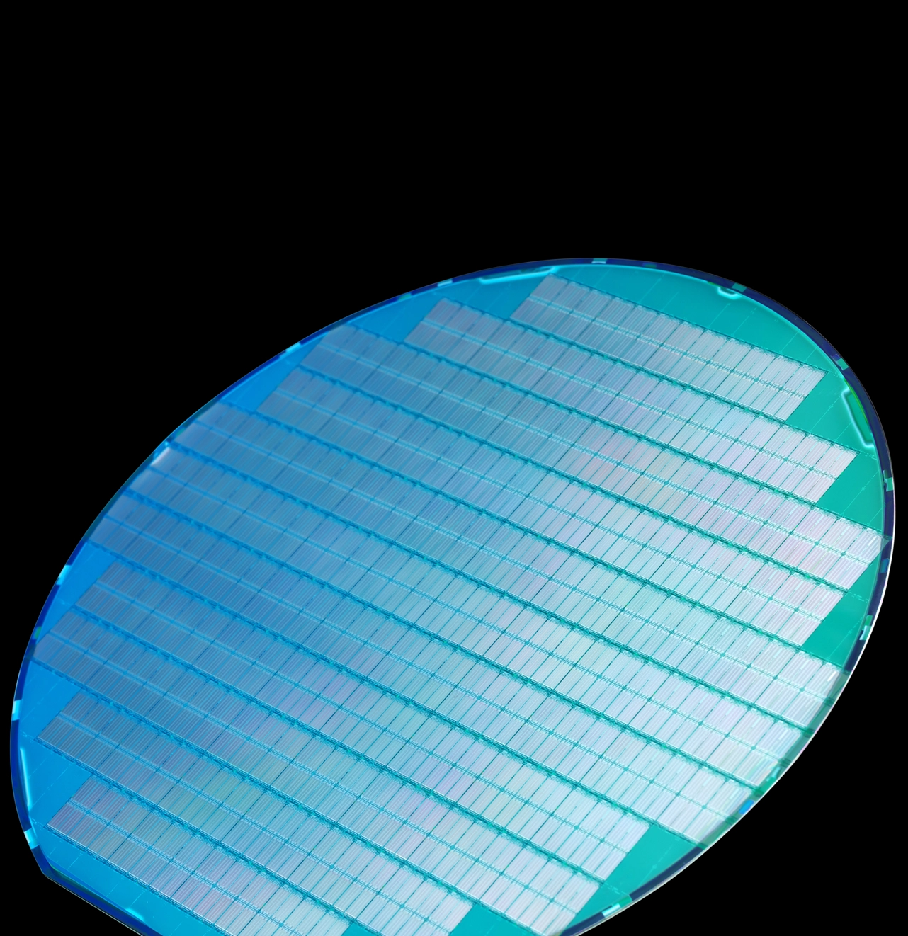
Industrial Cameras for Electronics
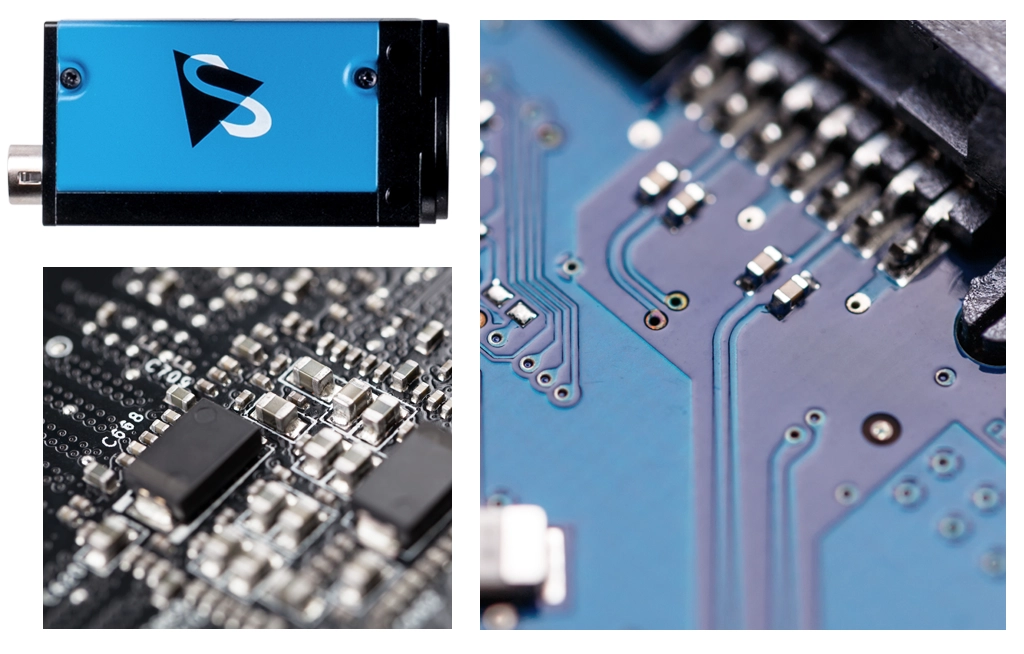
Since even micron-level flaws can cause functional failure in electronics manufacturing, accuracy and reliable imaging results are crucial. In order to identify defects invisible to the human eye, machine vision delivers the accuracy needed in applications such as wafer inspection, dicing, solder paste verification, and PCB assembly inspection. High-speed manufacturing lines, reflective surfaces, and sub-millimeter tolerances are some application challenges which demand industrial cameras with outstanding resolution, low noise, and precise triggering.
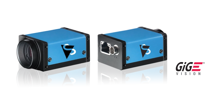
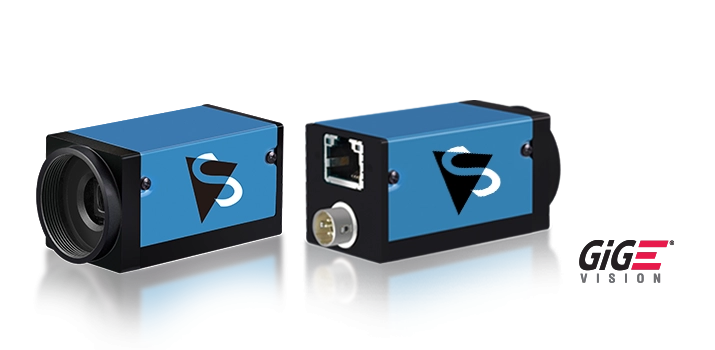
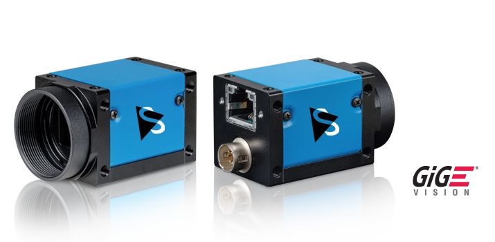
The Imaging Source's extensive portfolio of industrial and board-level cameras offers a large selection of color and monochrome options. The Imaging Source's industrial cameras provide the precision, stability, and integration flexibility required to satisfy the most exacting requirements of the electronics industry - from guided assembly to automated optical inspection (AOI), or surface mount technology (SMT) alignment.
Find ProductsApplications
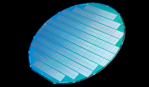
Wafer Surface and Defect Inspection
Detect particles, cracks, and surface irregularities using high-resolution industrial cameras for semiconductor wafer inspection tasks.
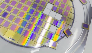
Dicing Saw Alignment and Crack Detection
Machine vision allows for precise saw alignment and detection of post-dicing microcracks for semiconductor processing lines.
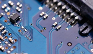
Solder Paste Inspection (SPI) for SMT Lines
Industrial cameras capture precise height, volume, and alignment data for solder paste inspection in high-speed SMT production lines.
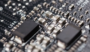
Automated Optical Inspection (AOI) for PCBs
Missing, misaligned, or defective components are reliably detected via machine vision for inline AOI in PCB and SMT inspection.

